Channel Length Modulation in Mosfet
6th symbol of slot 0 and slot 10time exis mapped on 72 subcarriers centered around DCfrequency axis. 1 shows the band diagrams of the n-channel TFET in the OFF and ON states.

Electronic Devices Mosfet Channel Length Modulation Clm Youtube
8 SATA3 1 Hyper M2 PCIe Gen4 x4 1 Hyper M2 PCIe Gen4 x4 SATA3 1.
. TFET is simply a gated p-i-n diode which is operating under reverse bias condition. In this circuit the V gs is the input signal applied between gate and source terminal and we know that the change in drain current is linearly proportional to V gsIn this model if you consider the effect of channel and modulation then there will also be an output resistance r0. A communication channel refers either to a physical transmission medium such as a wire.
Zadoff Chu sequence of length 63. In a MOSFET the source of carrier injection mechanism is thermal injection but a TFET utilizes band-to-band tunneling as a source carrier injection mechanism. Simulation results indicate that the MoS2 side-wall effective channel length approaches 0.
We do this by incorporating the incremental channel-length reduction into the original. Channel Length Modulation은 간단하게 L이 증가할 수록 그 현상이 줄어듬. N-channel MOSFET BSIM4SOI v431 Model.
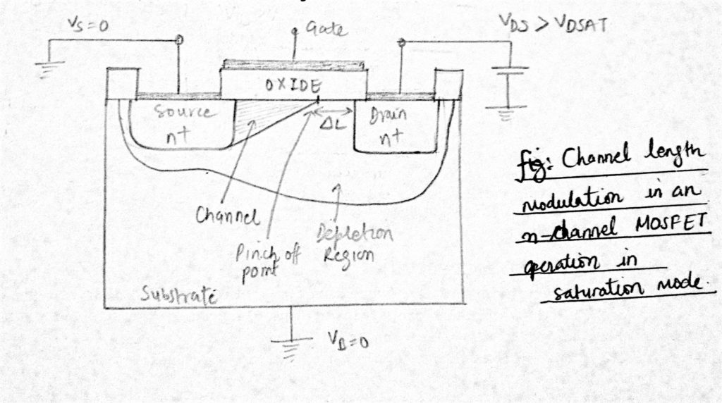
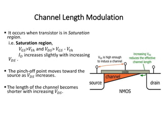
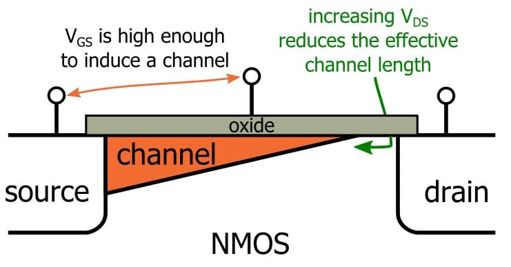
This is called channel-length modulation. WL is the ratio of Width and Length and λ is used for the modulation constant of channel length. 1R0 V D V G V SD V SG V T.
1 V can verify the modulation. Signal Full Form Direction Position Modulation Coding scheme Function. Hu MOSFET Modeling and BSIM3.
14 Layer Server-Grade Low-Loss PCB. The size of the antenna depends inversely on the highest frequency present in the. Since 2006 television broadcasting has switched to digital modulation digital television which uses image compression to transmit a television signal in a much smaller bandwidth.
However this can only happen if your house is already full channel-length modulation only happens when the device is in saturation If you start increasing your Vgs to the point of Vgss wellcops show up and shut you down. Chaparro Aydin Akan in Signals and Systems Using MATLAB Third Edition 2019 AM Communication System. 8 Power Phase Design 105A SPS Premium Power Choke.
Find the values required for W and R in order to establish a drain current of 01 mA and a voltage V D of 2 V. The longer the channel the less it is affected by the channel length modulation due to the increasing drain voltage. Underage drinking drug use etc.
White Solar Cells from Basics to Advanced Systems McGraw-Hill New York 267 pages 1983. These effects include in particular drain-induced barrier lowering velocity saturation quantum confinement and hot carrier degradation. Channel Length Modulation 은 λ 혹은 ro라는 수식으로 나타나게됨.
MOSFET Circuits Example The PMOS transistor has V T -2 V Kp 8 µAV2 L 10 µm λ 0. V GS V th and V DS are gate to source voltage. XXL Aluminum Alloy Heatsink.
If it is for a long length channel then as read in the Early Voltage section in the MOS transistor. λ 0 no channel length modulation. It is important to note that the inclusion of emitter resistors does not reduce the reduction in the output current I OUT caused by the finite beta of Q 1 and Q 2.
Pulse Width Modulation Generator. Consider the above current mirror circuit using MOSFET the MOSFET transistor M1 is in the saturation region as the V DS. Supports AMD Ryzen Threadripper PRO 3000WX5000WX Series Processors.
앞서 나온 수식들은 Ideal 한 경우이고 실제 Short channel로 갈수록 다른 Effect들이 생김. MOSFET TSNWFET with 15 nm length gate and 4 nm. 7 PCIe 40 x16.
Amplitude modulation AM communication systems arose from the need to send an acoustic signal a message over the airwaves using a reasonably sized antenna to radiate it. N-channel MOSFETBSIM4v5 v40 45 Model. So we need to modify the saturation-region drain-current expression to account for channel-length modulation.
Pulse Width Modulation Generator. In electronics short-channel effects occur in MOSFETs in which the channel length is comparable to the depletion layer widths of the source and drain junctions. UE first finds the primary synchronization signal PSS which is located in the last OFDM symbol of first time slot.
Defines Length of FET channel. Figure 115 Emitter degeneration included to boot output resistance. LEVEL Model type 1 2 or 3 1 L Channel length meters DEFL W Channel width meters DEFW LD Lateral diffusion length meters 0 WD Lateral diffusion width meters 0 VTO Zero-bias threshold voltage Volts 0 KP Transconductance AmpsVolts2 2E-5 GAMMA Bulk threshold parameter Volts12 0 PHI Surface potential Volts 06 LAMBDA Channel-length modulation Volts-1 0.
Thus channel-length modulation means that the saturation-region drain current will increase slightly as the drain-to-source voltage increases.
Channel Length Modulation In Mosfet Vlsi Design Buzztech

Mosfet Channel Length Modulation Explained Youtube
Threshold Voltage Channel Length Modulation
Mosfet Channel Length Modulation Technical Articles

L5 2 3channel Length Modulation Youtube

Drain End An Overview Sciencedirect Topics


Comments
Post a Comment